Chapter 3 Digital Logic Structures
Important
MOS transistor (Metal Oxide Semiconductor):
- n-type MOS transistor
- p-type MOS transistor
CMOS circuit:
- p-type + n-type MOS transistors
- to form logic gates
Transistors (晶体管): p/n-type MOS transistor
Transistor (switch) → combined to logic gates (logic functions) AND, OR, NOT → combined to build higher-level structures (Adder, multiplexer, decoder, register…) → combined to build processor (LC-3)
switch-based circuits (2 states): open/closed, on/off, voltage/no voltage.
switch open: 开关打开,no current
switch closed: 闭合, current flows
MOS: Metal oxide semiconductor
CMOS: Complementary Metal Oxide Semiconductor
- n-type MOS transistor:
gate positive (positive voltage): closed, short circuit (短路)
gate neg (zero voltage): open, open circuit (开路,断路)
if n-type is turned on (closed), pull down to 0 (GND).
#2 to the ground (GND, 0V)
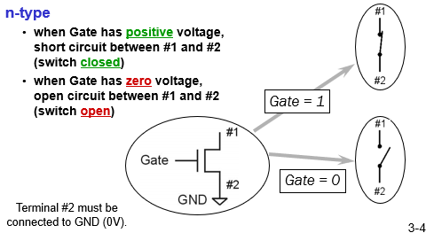
n-type: #2 to the GND
- p-type MOS transistor (complementary to n-type):
gate positive voltage: open, open circuit
gate 0 voltage: closed, short circuit
if p-type is turned on (closed), pull up to 2.9V (1).
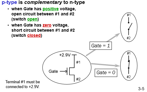
p-type: #1 to the +2.9V
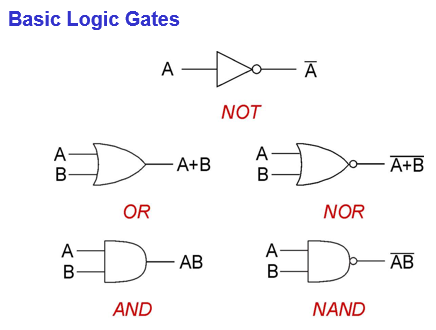
Logic Gates
Use MOS transistor switch to implement logic gates: AND, OR, NOT
CMOS: Complementary Metal Oxide Semiconductor, use both n-type and p-type MOS transistors.
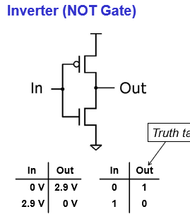
Inverter (NOT gate)
1 p-type (to the 2.9V #1) + 1 n-type (to the ground #2) transistor
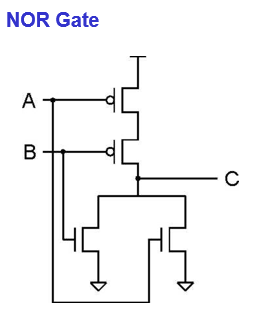
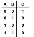
NOR gate (NOT OR)
if that circuit is open, then C will connect to the ground (0V);
if the circuit is closed, C will connect to both +2.9V and the ground, but resulting in 0V in C.
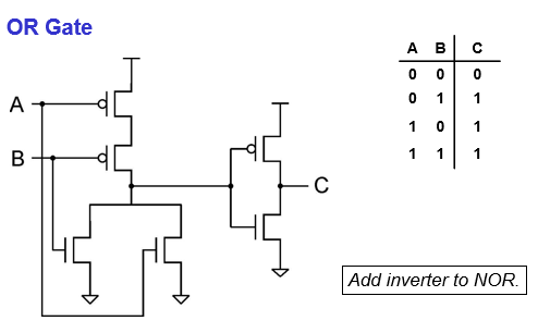
OR gate (Inverter / NOT + NOR)
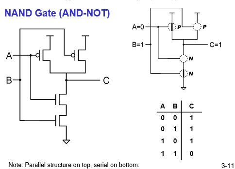
NAND Gate (NOT-AND)
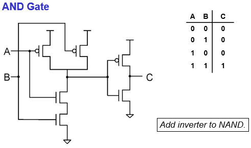
AND gate (NOT + NAND)
5 basic logic gates:
A new level of abstraction (implemented by MOS transistors / CMOS circuits)
- NOT
- AND
- NAND
- OR (A+B)
- NOR( )
Functions constructed by logic gates
- combinational logic circuit: stateless, output depends on the current inputs
- sequential logic circuit: stateful, output depends on the sequence of inputs (both current inputs and previous inputs)(previous inputs will be stored somehow). E.g., ticket counter.
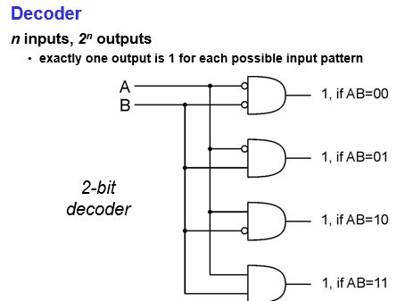
Combinational logic circuit: decoder, multiplexer, full adder
Sequential Logic circuit (storage elements): R-S latch, the gated D latch
Decoder
n inputs (n-bit), outputs (all possible bit patterns)
Multiplexer (MUX)
n-bit selector, inputs, one output
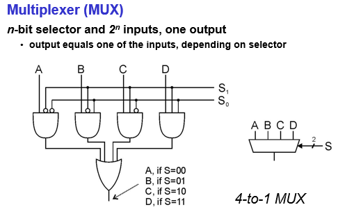
The output will be one of the inputs, depending on the bit pattern of the selector.
AND + OR
Full Adder
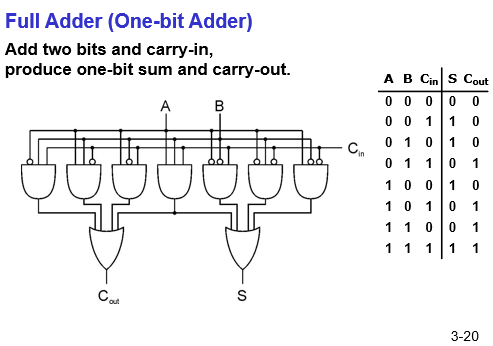
sum bit + carry over the next column
Logic completeness
Can implement any truth table by AND + OR + NOT.
Sequential logic circuit:
R-S latch (门闩)
Can store one bit of information ( 0 or 1 ).
Setting the latch (S): let the latch store a 1. (quiescent state / quiet state / holds the precious value)
Resetting the latch (R): let the latch store a 0. Take outputs as inputs to store values in the R-S latch.
R-S can be set to 1 as long as S = 0; can be set to 0 as long as R = 0; R and S are not allowed to set as 0 (be cleared) at the same time.
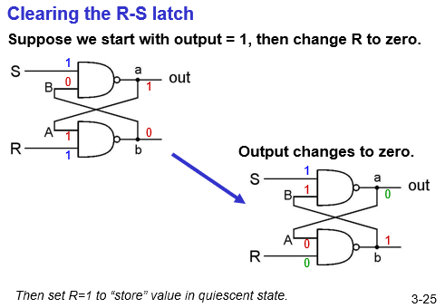
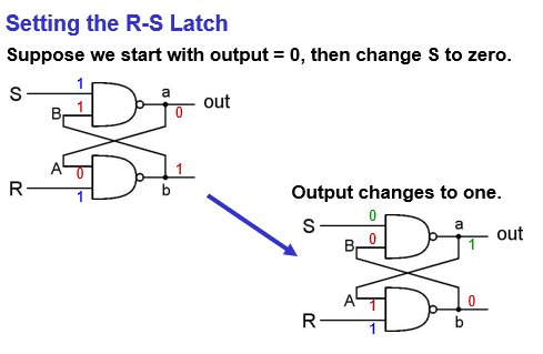
Summary of R-S Latch:
- R = S = 1, hold current value in the latch
- R = 0, S = 1, reset the value, as 0 (cleared)
- R = 1, S = 0, set the value as 1
- R = 0, S = 0, output depends on the electrical properties of gates. Don’t do it.
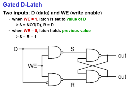
Gated D-Latch
Inputs: WE (write enable) + D (data)
if WE = 1, then set the R-S latch according to the value of D. Note: S = NOT(D), R = D
if WE = 0 → S = R = 1, the value of R-S latch remain unchanged.
Register
To store a multi-bit value.
Component:
- a collection of D-latches
- A common WE, Controlling all D-latches
when WE (write enable) = 1, n-bit value D is written to a register (into multiple R-S latches of those D latches)
However, in LC-3, the registers are implemented by flip-flops instead of gated D. See P95.
Register examples in LC-3: (P93)
- General purpose registers (in REG FILE block): R0 - R7
- Three single-bit condition code registers: N, Z, P
- Others: PC, MAR, MDR, IR…
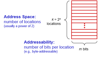
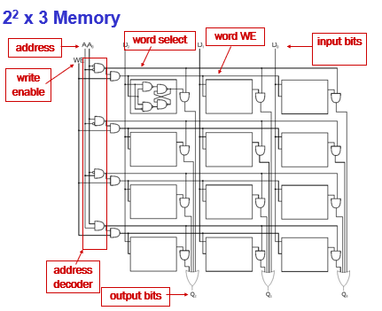
Memory
Outline
address space: number of locations, below
addressability: number of bits per location, m below
Component:
- Address Decoder (access certain line by address bits)
- word WE
- word select line
RAM, ROM
RAM: random access memory
volatile (不稳定的), temporarily stored the files that you are working on.
- SRAM: static RAM, fast
- DRAM: dynamic RAM, slower but denser
ROM: read-only memory
non-volatile, permanently stores instructions for the computer.
Sequential Logic Circuits
State Machine
A kind of Sequential circuit.
Purpose of building synchronous finite state machine: to direct the behavior of our system.
Recall: Markov Chain
State: A snapshot of all the relevant elements of the system at the moment the snapshot is taken.
state machine: Combines combinational logic + storage.
It can remember the state and changes output (and state) based on inputs and current state.
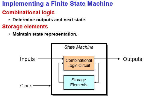
The stored value can act as the input of the combinational logic circuit.
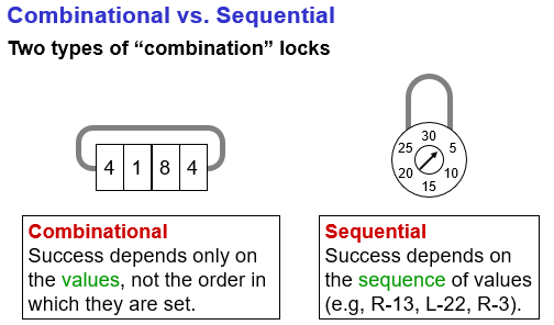
State diagram
states + actions → transition between states
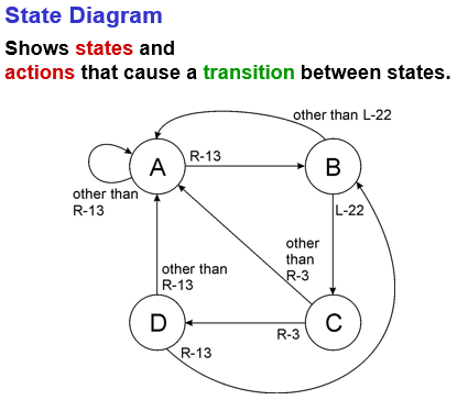
Components of state diagrams:
- a finite number of states
- a finite number of inputs
- a finite number of outputs
- state transitions
- explicit specification of what determines each external output value
Input triggers state transitions.
But the type of the transition is determined by input (e.g., the lock example) or input + current state or current state (no input, e.g., the traffic light without the switch)
The Clock
A clock circuit triggers transition from one state to the next. (The running of the state machine)
Master-Slave Flipflop (触发器)
A pair of gated D latches.
Problems of gated D latches as storage elements: the output of gated D latch would change the storage immediately in response to the input (given WE = 1). So the light would open and close fast and in repeat. We want storage elements to read the current state throughout the current clock cycle, and not write the next state values into the storage elements until the beginning of the next clock cycle.
Solution: Master-Slave flipflop, a pair of gated D latches
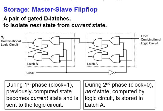
Each master-slave flipflop stores one state bit.
The number of storage elements (flipflops) needed (number of bits) is determined by the number of states (and representation of each states).
E.g., sequential lock, four states, → 2 bits (2 storage elements)
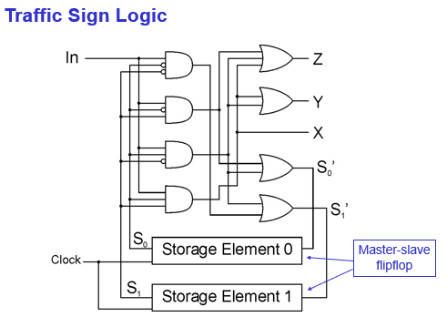
Traffic Sign Logic: combinational logic circuits + storage element (master-slave flipflop)
Data Path
From logic circuits to data path
Data path: all the logic used to process information.
P714, important LC-3 data path
Combinational logic of data path
- Decoders (convert instructions into control signals)
- Multiplexers: select specific input as output (AND + OR + selector)
- ALU: operations on data
Sequential logic of data path
- state machine: coordinate control signals and data movement
- registers and latches (R-S, gated D, master-slave flipflop): storage elements